For 60 years, the semiconductor industry followed one rule: make transistors smaller. Shrink the geometry, pack more into the same space, and performance improves. Moore’s Law. It worked for decades. Now it’s running into physics — at 3 nanometres, quantum tunnelling leaks current. The geometry approach is hitting a wall.
Huawei’s response, announced at IEEE ISCAS 2026 in Shanghai on May 25, is not to climb the wall. It’s to go around it.
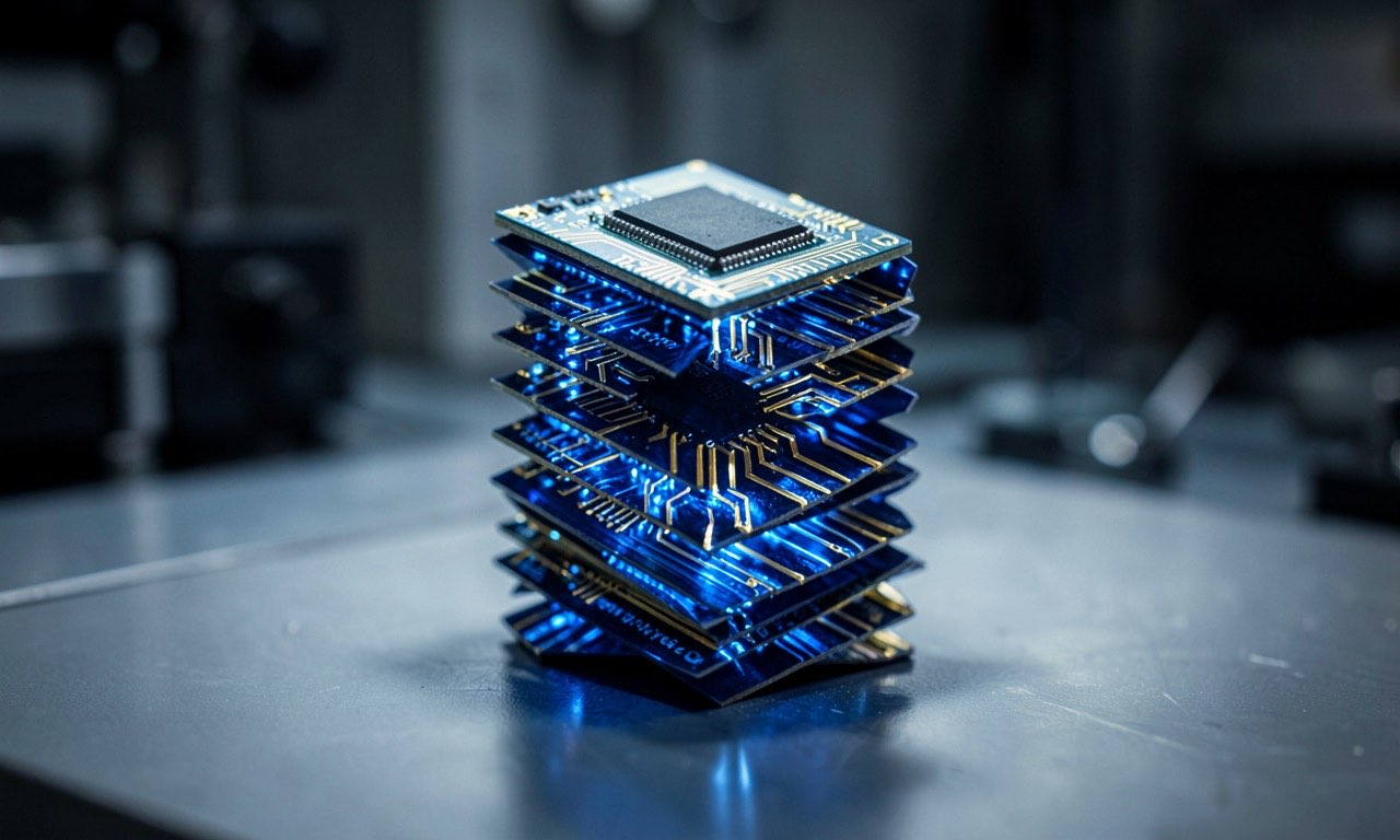
The Tau (τ) Scaling Law replaces geometric shrinking with time compression. Instead of making transistors smaller, Huawei makes signals travel shorter distances. The architecture is called LogicFolding — stacking transistors vertically and folding critical circuit paths across layers rather than spreading them flat. The result: higher transistor density, faster performance, and lower power consumption, all without the EUV lithography machines that the US and its allies have blocked China from accessing.
No ASML. No TSMC. No EUV. And 381 chips already shipped.
🔍 THE BOTTOM LINE
Huawei’s Tau Scaling Law may be the most consequential semiconductor announcement of the decade — not because of what it achieves technically, but because of what it makes irrelevant. If LogicFolding can deliver 1.4nm-equivalent transistor density by 2031 without EUV lithography, then the entire architecture of US chip sanctions — export controls on ASML machines, restrictions on TSMC foundry access, the CHIPS Act’s onshoring strategy — is potentially bypassed. The US spent years building a wall. Huawei built a tunnel underneath it. And Nvidia and Microsoft are now lobbying Washington to keep access to the Chinese market open, because they can see what’s coming.
The Problem With Shrinking
Moore’s Law has guided the semiconductor industry since 1965. Transistor counts double roughly every two years. Performance improves. Costs per transistor fall. The mechanism is geometric: shrink the features on the chip, and more transistors fit in the same area.
At advanced nodes — 5nm, 3nm, and below — this gets exponentially harder. Quantum tunnelling causes current leakage. Interconnect resistance rises. Power density creates heat problems. The cost of each new process node has ballooned: a leading-edge fab now costs $20 billion or more. Only three companies in the world — TSMC, Samsung, and Intel — can manufacture at the leading edge, and all of them depend on ASML’s EUV lithography machines.
This is the choke point the US identified. Control the EUV machines, and you control the pace of advanced chipmaking. The Netherlands agreed to restrict ASML exports to China. TSMC was barred from using US-designed tools to manufacture advanced chips for Chinese customers. The strategy was clear: keep China stuck on older process nodes, unable to produce the chips needed for frontier AI.
The Tau Scaling Law
Huawei’s answer is to redefine the problem. He Tingbo, president of Huawei’s semiconductor division, presented the Tau Scaling Law at IEEE ISCAS 2026. The principle is deceptively simple: instead of optimising for geometric size (making transistors smaller), optimise for time (making signals travel shorter distances).
EE Times explains the physics: the time constant τ can be mapped to RC delay — resistance times capacitance. Traditional geometric shrinking reduces RC delay as a side effect of making things smaller. Huawei’s approach targets RC delay directly, by shortening the physical path that signals travel through the circuit.
The key innovation is LogicFolding. Traditional chips lay circuits flat on a single plane. LogicFolding distributes critical path logic across vertical active layers, using hybrid bonding to connect them. The signal doesn’t travel as far. The RC delay drops. The transistor density increases — not because the transistors are smaller, but because the same area is used more efficiently through vertical stacking.
As He Tingbo put it: “The question is not ‘Can transistors continue to shrink?’ but ‘Can system time continue to shorten?’” Space and time, she said, are “two sides of the same coin.” Even if geometric scaling slows, time-level optimisation can continue.
The Receipts
This is not a lab experiment. Huawei has designed and mass-produced 381 chips based on the Tau Scaling Law over the past six years. The first consumer chip to use LogicFolding — the Kirin 2026 — launches this fall.
Tom’s Hardware reports the numbers: transistor density on the Kirin 2026 jumped from 155 million transistors per square millimetre to 238 million — a 55% increase in a single generation. Energy efficiency improved by approximately 41%. Maximum operating frequency increased by 13%, reaching 3.1 GHz. These are gains that would normally require a full process node shrink.
By 2031, Huawei targets transistor density equivalent to a 1.4nm process — comparable to what TSMC and Samsung expect to achieve with EUV lithography. Without a single EUV machine.
Huawei also addressed the system-level bottleneck. In large-scale AI computing, over 80% of energy consumption comes from data transport, not computation. Huawei’s Unified Bus architecture reduces inter-node communication latency from microseconds to approximately 100 nanoseconds — a 500-fold reduction — by eliminating protocol conversions and using memory-level semantics directly. The Hi-ONE optical interconnect engine provides 8 terabits per second of bandwidth per module, extending system connection distances to 100 metres. The goal: make a rack of AI chips behave as if it’s a single chip.
The Sanctions Paradox
The Tau Scaling Law is the hardware parallel to a pattern we’ve already seen in software.
DeepSeek trained its V3 model for approximately $6 million on older A100 chips — chips the US allowed China to buy before tighter restrictions kicked in. US export controls on cutting-edge hardware were supposed to slow Chinese AI progress. Instead, they accelerated efficiency innovation. DeepSeek couldn’t buy H100s, so it figured out how to do more with less. The constraint became the catalyst.
Huawei’s τ Scaling is the same story in silicon. The US blocked EUV access. Huawei couldn’t follow the geometric scaling path that TSMC, Samsung, and Intel are on. So it found a different path entirely — one that doesn’t need EUV at all.
SiliconANGLE framed it bluntly: Huawei “unveiled a sanctions-busting chip architecture.” That’s one reading. Another is that when you wall off the obvious path, the blocked party has a powerful incentive to find a better one. The US may have inadvertently pushed Huawei toward an innovation that wouldn’t have been pursued if EUV had been available.
This doesn’t mean the sanctions were wrong. From a US national security perspective, slowing China’s access to cutting-edge chips was a rational strategy — and it did buy time. But the time has been used. The wall is still standing. The tunnel is already through.
Why Nvidia and Microsoft Are Worried
The chip breakthrough connects directly to another story playing out this week: Nvidia and Microsoft are lobbying Washington to keep open-weight AI models legal and to avoid cutting off access to Chinese AI technology.
CNBC reported that Nvidia, Microsoft, and Meta are warning against overregulating open-weight models. The stated reason is competitiveness. The commercial reason is simpler: Nvidia sells GPUs and Microsoft sells Azure credits. If US policy walls off the Chinese AI ecosystem, those companies lose access to one of the largest markets for AI compute on the planet.
Jensen Huang made it personal. On July 24, in his first-ever post on X, Nvidia’s CEO shared an open letter on why open models matter. “AI will transform every industry, power every company, and be built by every country,” he wrote. “Open models strengthen safety and cybersecurity, accelerate innovation and diffusion, and enable sovereignty. The world needs both frontier closed models and frontier open models.” The post drew 28.3 million views. It was the CEO of the world’s most valuable AI hardware company using his first public statement on the platform to argue against the restrictionist camp in Washington — and framing open models as a sovereignty issue, the exact language that appeals to the Global South countries China is courting through WAICO.
The commercial subtext was not lost on observers. One of the most-liked replies summarised it: “tl;dr: ‘GPU consumption should be increased, not decreased’ — GPU seller.” Jensen Huang is right that open models strengthen safety and diffusion. He’s also right that the world needs both open and closed models. But Nvidia’s commercial interest and the open-weight argument happen to align perfectly — and Huawei’s τ Scaling makes that alignment more urgent than ever.
Within hours, Elon Musk endorsed Jensen’s post with a simple: “This has my full support. Jensen is right.” 4.2 million views. Two of the most powerful technology CEOs in the world — the owner of X and xAI, the CEO of Nvidia — publicly aligning on open models on the same day. The open-weights coalition is no longer just a lobbying effort. It’s a public stand by the industry’s most influential figures, and Washington is watching.
Huawei’s τ Scaling makes this lobbying more urgent — and more complicated. If China can produce advanced chips without Western technology, then the US has lost its primary leverage. The only remaining tool is software restrictions — banning Chinese AI models, restricting access to US frontier models. But as the Kimi K3 release demonstrated, China’s open-weight models are already competitive and already on the internet. You can’t put them back in the box.
The uncomfortable reality for Washington: hardware sanctions were the strong hand. If that hand is weakening, the software restrictions being discussed now — banning Chinese models, restricting open weights — are a weaker substitute. And the companies that make the chips and run the clouds are telling policymakers not to play it. When Jensen Huang’s first act on a platform with 28 million eyes is to advocate for open models, the signal to Washington is clear: the industry doesn’t want the doors to close.
What This Means for the Rest of the World
If the bifurcation between US and Chinese technology stacks is accelerating — and we argued this week that it is — then Huawei’s τ Scaling has implications beyond the US-China rivalry.
For countries building AI infrastructure, the choice of stack just got more complicated. The US stack assumes access to TSMC-manufactured chips on ASML-equipped processes. The Chinese stack now includes a path to advanced silicon that doesn’t depend on either. For countries in the Global South, the Pacific, and Southeast Asia — where WAICO’s 29 signatories are building AI infrastructure — the Chinese stack is becoming more self-sufficient, not less.
For New Zealand, the implications are the same as those we explored in the Iran/AWS data center story: when AI infrastructure becomes a national asset rather than a commercial product, countries without their own compute are dependent on whichever stack they align with. The difference now is that the Chinese stack may not need Western components at all.
This also connects to the ASML capacity expansion story we covered earlier this month. ASML is raising its EUV capacity forecast — the West is investing heavily in the lithography path. That investment may be sound. But it’s a bet on one approach to chip advancement. Huawei is betting on another.
The Skeptical View
The τ Scaling claims deserve scrutiny. Huawei’s numbers are self-reported. The 1.4nm-equivalent target is for 2031 — five years out. LogicFolding has been validated in one consumer chip (Kirin 2026), not yet at the scale required for data centre AI accelerators. The hybrid bonding process has its own manufacturing challenges, and yield rates are not disclosed.
There are also honest questions about whether “1.4nm-equivalent” means what it sounds like. Transistor density is one metric. Performance, power efficiency, and manufacturability at scale are different challenges. TSMC and Samsung are not standing still — they have their own 3D stacking technologies (TSMC’s SoIC, Intel’s Foveros) that pursue similar goals through different means.
The point is not that Huawei has definitively leapt ahead. The point is that the sanctions strategy assumed China would be stuck on older process nodes for years. That assumption now looks wrong. Whether τ Scaling delivers on its 2031 targets or not, the direction is clear: China is building a parallel semiconductor path that doesn’t depend on the Western supply chain.
❓ FAQ
What is the Tau Scaling Law? A principle proposed by Huawei that replaces geometric scaling (making transistors smaller) with time scaling (making signals travel shorter distances). The time constant τ maps to RC delay in circuits. By reducing signal path length through vertical stacking, Huawei claims it can improve transistor density and performance without shrinking transistors.
What is LogicFolding? Huawei’s chip architecture that distributes critical circuit paths across vertical active layers instead of laying them flat. This shortens signal propagation distance, reduces RC delay, and increases transistor density. It requires hybrid bonding technology but does not require EUV lithography.
Does this really make US sanctions obsolete? Not immediately. Huawei’s 1.4nm-equivalent target is for 2031. The Kirin 2026 is a smartphone chip, not a data centre AI accelerator. But the direction — a viable semiconductor path that doesn’t depend on ASML, TSMC, or Western technology — potentially undermines the foundation of the chip export control strategy.
How does this connect to the AI nationalisation story? Huawei’s τ Scaling is the hardware parallel to DeepSeek’s software efficiency. Both prove the same point: US constraints forced innovation rather than blocking it. Together, they suggest China’s AI stack is becoming self-sufficient at both the hardware and software layers — which is the trajectory we described in our analysis of China’s AI playbook.
What about TSMC’s own 3D stacking? TSMC, Intel, and Samsung all have vertical stacking technologies (SoIC, Foveros, X-Cube). The difference is that these are additive — they complement EUV lithography. Huawei’s approach is designed to substitute for it entirely. Whether that’s achievable at the same performance level is an open question.
📰 Sources
- Huawei — Presents the Tau (τ) Scaling Law at IEEE ISCAS 2026
- EE Times — From Shrinking Transistors to Compressing Time: Deciphering Huawei’s τ Law
- Tom’s Hardware — Huawei claims sanctions-busting breakthrough with 1.4nm-class chips by 2031
- SiliconANGLE — China’s Huawei unveils new sanctions-busting chip architecture
- CNBC — Nvidia, Microsoft, Meta warn against overregulating open-weight models
- SoyaCincau — Tau Scaling: Huawei’s radical architectural approach to overcome US sanctions
- Jensen Huang on X — First post: open models letter (July 24, 2026)
- Elon Musk on X — Endorsement of Jensen Huang’s open models letter
— CJ Murden, editor of Singularity.Kiwi. Former digital technologies teacher, author of AI-focused books. Writing with a New Zealand focus.